
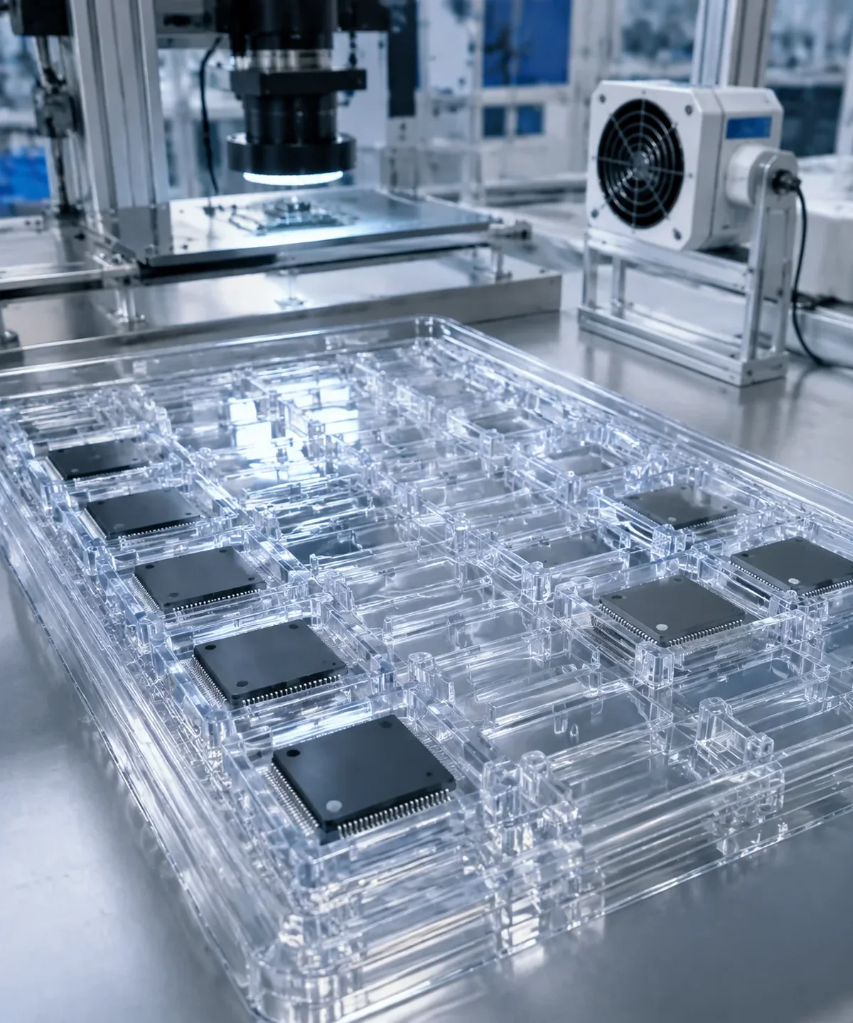
The short answer: three different failures require three kinds of evidence
Transparent antistatic chip tray risk has three layers. First, a coating or migrating additive can decay after wiping, washing or low-humidity exposure. Second, temperature, shear, flow length and weld lines can create electrical and optical variation across the molded tray. Third, a device can experience a charged device model event even when tray resistance remains inside its project range. Material screening, molded-part validation and ESD-system assessment are therefore separate requirements.
| Failure layer | Typical signal | Insufficient evidence | Evidence to add |
|---|---|---|---|
| Surface decay | Resistance rises after low humidity or cleaning | One shipment reading | Before-and-after humidity, wipe, wash and storage tests |
| Molding variation | Flow end, thin wall or weld line becomes abnormal | One point on a standard plaque | Multiple locations and batches of the real tray |
| CDM system risk | A charged device rapidly discharges to a conductor | Assuming lower tray resistance is always safer | Device sensitivity, low charging, grounding and EPA controls |
Normalize terminology before comparing data. Surface resistance is reported in Ω, surface resistivity is commonly reported in Ω/□, and volume resistivity is reported in Ω·cm. The method, electrode, sample condition, temperature, humidity and read time must also match.
Failure 1: surface performance decays during cleaning and low-humidity use
Migrating antistatic additives move toward the polymer surface and may rely on absorbed moisture to lower resistance. Wiping and washing can remove surface material, while dry air can reduce the moisture available to form a conductive path. A coating faces a related limitation: once the functional surface is worn, the ordinary polymer beneath it may not provide the same static-control performance.
No fixed number of months describes every formulation. Wall thickness, cleaner, wipe load, baking temperature, humidity and use frequency all change the outcome. A defensible report compares the same electrical metric before and after a defined exposure instead of relying on “permanent” or “long-lasting” wording.
An existing Clearastatic medical-monitor panel record provides cross-application durability evidence. A coated clear ABS panel was wiped repeatedly with 75% alcohol in an ICU and developed static-related dust attraction in frequently wiped areas after three to six months. After changing to intrinsic antistatic ABS and revalidating, the project part remained within 10⁸-10⁹ Ω/□ surface resistivity after 500 alcohol wipes. This is evidence for one confidential part and test condition, not a universal chip-tray service-life claim.
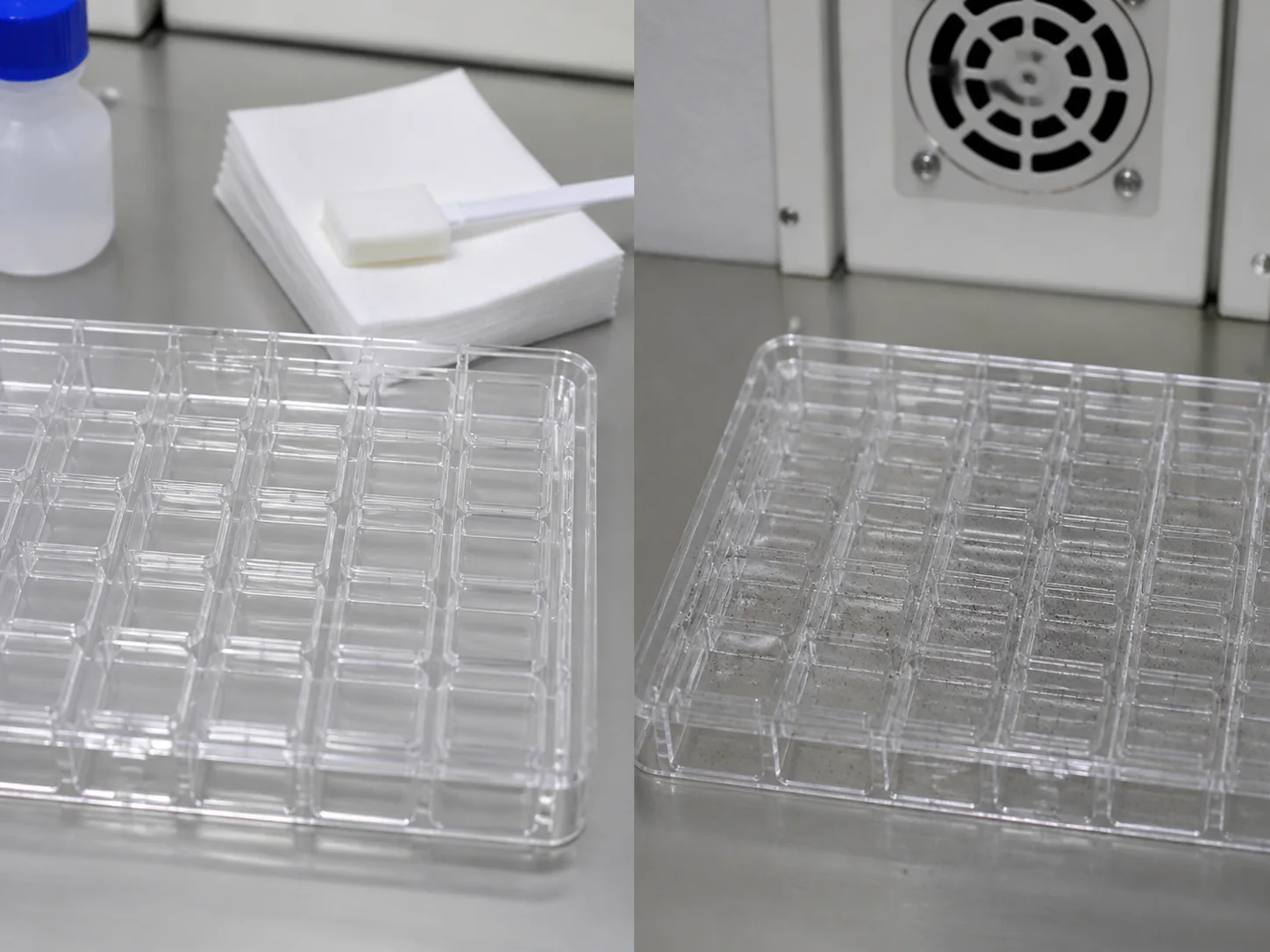
Failure 2: molding creates electrical and optical variation across one tray
A passing data sheet does not qualify a tray. As pellets become a thin-wall, multi-cavity or long-flow component, the material experiences drying, plasticization, shear, splitting, weld formation and rapid cooling. The gate, flow end, weld line and chip-contact area can produce different electrical results. A transparent tray can also show splay, bubbles, flow marks or local haze at the same time.
Carbon black, carbon fiber and other filled systems can be affected by filler orientation, agglomeration and weld interfaces. A polymeric intrinsic antistatic system does not have the same rigid-filler orientation mechanism, but drying, melt temperature, shear, wall thickness and cooling can still change phase structure, appearance and electrical distribution. Intrinsic modification therefore does not remove the need for molded-part testing.
| Process item | DGK-ABS KJD890TM starting reference | Record on the machine |
|---|---|---|
| Drying | 85°C for 4-5 hours | Dryer, actual material temperature, dew point and transfer delay |
| Injection temperature | 195-210°C | Zone settings, melt condition and residence time |
| Mold temperature | 70°C starting reference | Measured temperature on both halves and local variation |
| Part locations | Gate, middle, end and weld area at minimum | Thickness, direction, surface condition and point identifier |
These are trial starting points, not mandatory settings for every mold. Tray size, flow-length ratio, gate design, colorant, machine and target resistance all affect the final process window.
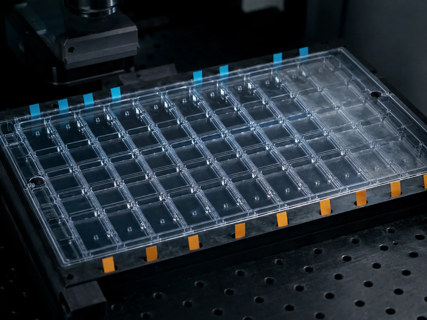
Failure 3: tray resistance passes, but CDM risk remains
The charged device model describes an event in which a device accumulates charge and then rapidly discharges to a conductive surface at lower potential. A chip can charge during feeding, vibration, contact and separation. When a pin contacts a metal fixture, the discharge may last less than one nanosecond and its peak current may reach several amperes or more. The outcome depends on the device, capacitance, charge voltage, package and contact conditions.
Tray resistance is therefore neither “the lower the better” nor a complete CDM solution. The ESD Association notes that resistance or resistivity alone does not predict low-charging behavior. Packaging also needs dissipative, groundable or discharge-shielding properties according to whether it is used inside or outside an ESD protected area. HBM and CDM sensitivity should be included in the control plan.
Validate the material and system separately. On the material side, check surface electrical performance, charging tendency and durability. On the system side, review device sensitivity, automated handling, grounding and equipotential bonding, ionization where needed, and packaging function across the EPA boundary. Simply changing to a more conductive plastic can hide the real hazard source.

Project evidence: a trial that exposed a local molding defect
Case-source note: the following figures come from an anonymized Clearastatic medical-monitor panel project. It was not a chip tray, but it used DGK-ABS KJD890TM and shows why a transparent static-control molded part needs multi-location and process validation.
The first trial used 85°C drying for four to five hours, 195-210°C injection temperature and a 70°C mold temperature. The molded part reached 87% light transmission and 3.2×10⁸ Ω/□ surface resistivity, but a slight cloudy area appeared near a 1.2 mm thin-wall flow end. The team raised mold temperature to 75°C and used a slow-medium-slow filling profile. The cloudy area disappeared in the second trial.
The lesson is not to copy 75°C into every tray process. It is to show that average data can pass while a local area fails. Define critical locations first, then relate electrical, optical, dimensional and appearance results to each process revision.
| Validation object | First-trial result | Adjustment or conclusion |
|---|---|---|
| Overall transmission | 87% | Met this project's target |
| Surface resistivity | 3.2×10⁸ Ω/□ | Met this project's range |
| 1.2 mm thin-wall flow end | Slight cloudiness | Removed after mold-temperature and fill-profile changes |
| Durability retest | 10⁸-10⁹ Ω/□ after 500 alcohol wipes | Applicable only to the documented project conditions |

Acceptance checklist for a transparent antistatic chip tray
| Level | Required record | Recommended decision rule |
|---|---|---|
| Material | Grade, batch, metric, unit, method and electrode | Separate surface resistance from surface resistivity |
| Optical | Thickness, transmission, haze, color and defects | Set limits from vision-system or human-inspection needs |
| Molded tray | Gate, middle, flow end, weld line and contact area | Report distribution rather than only an average |
| Environment | Temperature, humidity, conditioning and read time | Include the lowest relevant plant humidity |
| Durability | Cleaner, cycles, temperature, baking and storage | Compare before and after with the same method |
| ESD system | Device HBM/CDM rating, EPA location, grounding and ionization | Assess the real handling path |
| Production | Batch sampling, point IDs, exceptions and change records | Trend results and preserve traceability |
For initial screening, cross-check the publicly available transparent antistatic ABS data, then build a real-tray plan around material testing, samples and production introduction. Transparent ABS suits applications that require internal visibility without high-temperature baking; confirm that the actual process remains within the material's temperature limits.
Data notes and scope
Material parameters draw on Clearastatic DGK-ABS KJD890TM information and publicly available product data reviewed on September 6, 2026. Surface resistance and surface resistivity are identified separately. The case evidence comes from anonymized Clearastatic medical-monitor panel molding, wiping, low-humidity, delivery and after-sales records.
This article supports material screening and validation planning. It is not a semiconductor reliability certification or a project-specific ESD acceptance result. The project owner should confirm the applicable editions and limits of ANSI/ESD S541, ANSI/ESD S20.20, IEC 61340-5-1 and customer specifications.